Main Processor: VIA Eden, 800.0 MHz
Math Co-Processor: Internal
Bus Type: PCI (V2.10) + AGP 8X (V3.0)
Mainboard Model: CN900-8237R
Mainboard Chipset: VIA P4M800 Pro/CE/CN700
First Level Cache: Instruction: 64 KBytes, Data: 64 KBytes
Second Level Cache: Integrated: 128 KBytes
System Memory Size: 640 KBytes
Extended Memory Size: 192,640 KBytes Total: 189 MBytes
Shadow+Special RAM Size: 256 KBytes
Machine Type: IBM PC AT
Computer Name: WYSE V CLASS L
BIOS Manufacturer: Phoenix - AwardBIOS v6.00PG [07/21/08]
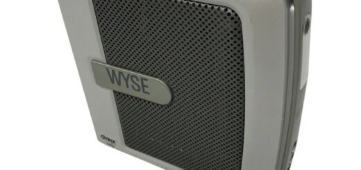
System Manufacturer: WYSE
Product Name: V CLASS L
Product Version: Rev: 1.18
Product Serial Number: 6WQ0H945240
Mainboard Manufacturer: VIA
Mainboard Name: CN900-8237R
Mainboard Version:
Mainboard Serial Number:
RAM
Error Detecting Method: None
Error Correction: None
Supported Interleave: 8-Way
Current Interleave: 4-Way
Max. Memory Module Size: 1024 MBytes
Supported Memory Speed: 70 ns, 60 ns
Supported Memory Type: DIMM, SDRAM
Supported Memory Voltage: 2.9 V
Associated Memory Slots: 1
Port Type:                Unknown
Internal Reference:       PRIMARY IDE
Internal Connector Type:  On Board IDE
External Reference:       Unknown
External Connector Type:  None

Port Type:                Unknown
Internal Reference:       SECONDARY IDE
Internal Connector Type:  On Board IDE
External Reference:       Unknown
External Connector Type:  None

Port Type:                8251 FIFO Compatible
Internal Reference:       FDD
Internal Connector Type:  On Board Floppy
External Reference:       Unknown
External Connector Type:  None

Port Type:                Serial Port 16450 Compatible
Internal Reference:       COM1
Internal Connector Type:  9 Pin Dual Inline (pin 10 cut)
External Reference:
External Connector Type:  DB-9 pin male

Port Type:                Serial Port 16450 Compatible
Internal Reference:       COM2
Internal Connector Type:  9 Pin Dual Inline (pin 10 cut)
External Reference:
External Connector Type:  DB-9 pin male

Port Type:                Parallel Port ECP/EPP
Internal Reference:       LPT1
Internal Connector Type:  DB25 pin female
External Reference:
External Connector Type:  DB25 pin female

Port Type:                Keyboard Port
Internal Reference:       Keyboard
Internal Connector Type:  PS/2
External Reference:
External Connector Type:  PS/2

Port Type:                Mouse Port
Internal Reference:       PS/2 Mouse
Internal Connector Type:  PS/2
External Reference:
External Connector Type:  PS/2

Port Type:                USB
Internal Reference:       Unknown
Internal Connector Type:  None
External Reference:       USB0
External Connector Type:  Unknown
CPU ID:                   000006D0  (CPUID) ù 00000000  (Ext. CPUID)
CPU Stepping:             Esther (C5R)
CPU Vendor Name:          VIA Eden Processor  800MHz

CPU Current:              800.0 MHz = 8.00 x 100.0 MHz @ 0.8440 V
Number of CPU Cores:      1
Number of Logical CPUs:   1

Instruction TLB:          8-way set associative, 128 entries
Data TLB:                 8-way set associative, 128 entries

CPU Update Revision:      N/A
Multi-Processor System:   Present (V1.4)

P.I. ROM:                 Not Present

Processor Manufacturer:   VIA
Processor Version:        VIA Eden
External Clock:           100 MHz
Maximum Clock:            800 MHz
Current Clock:            800 MHz
CPU Socket:               Populated
CPU Status:               Enabled
Processor Type:           Central Processor
Processor Voltage:        2.3 V
Processor Upgrade:        None
Socket Designation:       NanoBGA2
                         FPU on Chip
                             Enhanced Virtual-86 Mode
                             I/O Breakpoints
                             Page Size Extensions
                             Time Stamp Counter
                             Pentium-style Model Specific Registers
                             Physical Address Extension
                             Machine Check Exception
                             CMPXCHG8B Instruction
                             APIC On Chip / PGE (AMD)
                             Fast System Call
                             Memory Type Range Registers
                             Page Global Feature
                          x   Machine Check Architecture
                             CMOV Instruction
                             Page Attribute Table
                          x   36-bit Page Size Extensions
                          x   Processor Number
                             CLFLUSH Instruction
                          x   Debug Trace and EMON Store
                             Internal ACPI Support
                             MMX~ Technology
                             Fast FP Save/Restore (IA MMX-2)
                             Streaming SIMD Extensions
                             Streaming SIMD Extensions 2
                          x   Self-Snoop
                          x   Multi-Threading Capable
                             Automatic Clock Control
                          x   IA-64 Processor
                             Signal Break on FERR
                             Streaming SIMD Extensions 3
                          x   Carryless Multiplication (PCLMULQDQ)
                          x   MONITOR/MWAIT Support
                          x   Supplemental Streaming SIMD Extensions 3
                          x   FMA Extension
                          x   CMPXCHG16B Support
                          x   Streaming SIMD Extensions 4.1
                          x   Streaming SIMD Extensions 4.2
                          x   x2APIC
                          x   POPCNT Instruction
                          x   AES Cryptography Support
                          x   XSAVE/XRSTOR/XSETBV/XGETBV Instructions
                          x   XGETBV/XSETBV OS Enabled
                          x   AVX Support
                          x   Half-Precision Convert (CVT16)
                          x   FPU on Chip
                          x   Enhanced Virtual-86 Mode
                          x   I/O Breakpoints
                          x   Page Size Extensions
                          x   Time Stamp Counter
                          x   IDT-style Model Specific Registers
                          x   Machine Check Exception
                          x   CMPXCHG8B Instruction
                          x   SYSCALL and SYSRET Instructions
                          x   Page Global Feature
                          x   Machine Check Architecture
                          x   CMOV Instruction
                          x   FCMOV Instruction
                          x   MMX~ Technology
                          x   3DNow!~ Technology
Segment Size    BIOS Extensions

 C000h    56K   VIA/S3 Unichrome Pro Integrated Video Adapter
 D800h     8K   VIA VT6102 Rhine II Fast Ethernet Adapter           [PnP]


Flash BIOS:               <Skipped>

BIOS32 services:          Present
Plug-and-Play support:    Present (V1.0)
APM support:              Present (V1.2)
ACPI support:             Present

BIOS Vendor:              VIA Technologies, INC.
BIOS Version:             Rev: 1.18
BIOS Release Date:        07/21/2008
BIOS Start Segment:       E000
BIOS Size:                512 KBytes
ISA Support:              Present
MCA Support:              Not Present
EISA Support:             Not Present
PCI Support:              Present
PC Card (PCMCIA) Support: Not Present
Plug-and-Play Support:    Present
APM Support:              Present
Flash BIOS:               Present
BIOS Shadow:              Present
VL-VESA Support:          Not Present
ESCD Support:             Present
Boot from CD:             Present
Selectable Boot:          Not Present
BIOS ROM Socketed:        Not Present
Boot from PC Card:        Not Present
EDD Support:              Not Present
NEC PC-98 Support:        Not Present
Vendor ID:                OEM00000
Product ID:               PROD00000000

Present CPU(s):           CPU ID: 06D0 (Bootstrap)
                          CPU ID: 0000


Present Bus(es):          PCI
                          PCI
                          ISA


Present APIC(s):          Base Address: FEC00000
Bus Type                  Bus Number

PCI                       0
AGP                       1
PnP Capable Devices:      None
PnP System Devices:       12 Nodes

PnP ESCD Support:         Present (V2.1)
PnP DMI Support:          Present (V2.3)
Node 0: PNP0000 – Programmable Interrupt Controller
Device ID:                PNP0000 (Programmable Interrupt Controller)
Device Type Code:         080000
Device Features:          [x Disableable] [x Configurable] [x Removable]
Device Capabilities:      [x IPL] [x Input] [x Output] [x Docking]
Supported IRQ(s):         2
I/O Port(s):              0020
I/O Port(s):              00A0
Node 1: PNP0200 – DMA Controller
Device ID:                PNP0200 (DMA Controller)
Device Type Code:         080100
Device Features:          [x Disableable] [x Configurable] [x Removable]
Device Capabilities:      [x IPL] [x Input] [x Output] [x Docking]
Supported DMA(s):         4
I/O Port(s):              0000
I/O Port(s):              0081
I/O Port(s):              0087
I/O Port(s):              0089
I/O Port(s):              008F
I/O Port(s):              00C0
Node 2: PNP0100 – System Timer
Device ID:                PNP0100 (System Timer)
Device Type Code:         080201
Device Features:          [x Disableable] [x Configurable] [x Removable]
Device Capabilities:      [x IPL] [x Input] [x Output] [x Docking]
Supported IRQ(s):         0
I/O Port(s):              0040
Node 3: PNP0B00 – RealTime Clock
Device ID:                PNP0B00 (RealTime Clock)
Device Type Code:         080300
Device Features:          [x Disableable] [x Configurable] [x Removable]
Device Capabilities:      [x IPL] [x Input] [x Output] [x Docking]
Supported IRQ(s):         8
I/O Port(s):              0070
Node 4: PNP0303 – 101/102-Key or MS Natural Keyboard
Device ID:                PNP0303 (101/102-Key or MS Natural Keyboard)
Device Type Code:         090000
Device Features:          [x Disableable] [x Configurable] [x Removable]
Device Capabilities:      [x IPL] [ Input] [x Output] [x Docking]
Supported IRQ(s):         1
I/O Port(s):              0060
I/O Port(s):              0064
Node 5: PNP0800 – PC Speaker
Device ID:                PNP0800 (PC Speaker)
Device Type Code:         088000
Device Features:          [x Disableable] [x Configurable] [x Removable]
Device Capabilities:      [x IPL] [x Input] [x Output] [x Docking]
I/O Port(s):              0061
Node 6: PNP0C04 – Numeric Data Processor
Device ID:                PNP0C04 (Numeric Data Processor)
Device Type Code:         0B0100
Device Features:          [x Disableable] [x Configurable] [x Removable]
Device Capabilities:      [x IPL] [x Input] [x Output] [x Docking]
Supported IRQ(s):         13
I/O Port(s):              00F0
Node 7: PNP0C01 – System Board Extension
Device ID:                PNP0C01 (System Board Extension)
Device Type Code:         050000
Device Features:          [x Disableable] [x Configurable] [x Removable]
Device Capabilities:      [x IPL] [x Input] [x Output] [x Docking]
Memory Location (fixed):  00000000-0009FFFF (RAM)
Memory Location (fixed):  FFFE0000-FFFFFFFF (ROM)
Memory Location (fixed):  FEC00000-FEC0FFFF (ROM)
Memory Location (fixed):  FEE00000-FEE0FFFF (ROM)
Memory Location (fixed):  00100000-00FFFFFF (RAM)
Node 8: PNP0C02 – Motherboard Resources
Device ID:                PNP0C02 (Motherboard Resources)
Device Type Code:         088000
Device Features:          [x Disableable] [x Configurable] [x Removable]
Device Capabilities:      [x IPL] [x Input] [x Output] [x Docking]
Memory Location (fixed):  000F0000-000F3FFF (ROM)
Memory Location (fixed):  000F4000-000F7FFF (ROM)
Memory Location (fixed):  000F8000-000FFFFF (ROM)
Memory Location (fixed):  000DA000-000DBFFF (ROM)
Node 9: PNP0A03 – PCI Bus
Device ID:                PNP0A03 (PCI Bus)
Device Type Code:         060400
Device Features:          [x Disableable] [x Configurable] [x Removable]
Device Capabilities:      [x IPL] [x Input] [x Output] [x Docking]
I/O Port(s):              04D0
I/O Port(s):              0CF8
Node 12: PNP0400 – Parallel Port
Device ID:                PNP0400 (Parallel Port)
Device Type Code:         070100
Device Features:          [ Disableable] [ Configurable] [x Removable]
Device Capabilities:      [x IPL] [x Input] [x Output] [x Docking]
Supported IRQ(s):         7
I/O Port(s):              0378
Node 14: PNP0501 – 16550A-compatible UART Serial Port
Device ID:                PNP0501 (16550A-compatible UART Serial Port)
Device Type Code:         070002
Device Features:          [ Disableable] [ Configurable] [x Removable]
Device Capabilities:      [x IPL] [x Input] [x Output] [x Docking]
Supported IRQ(s):         3
I/O Port(s):              02F8
Bus Dev Fun   Device

 0   0   0    VIA P4M800 Pro/CE/CN700/VN800 Chipset - AGP Controller
 0   0   1    VIA P4M800 Pro/CE/CN700/VN800 Chipset - Error Reporting
 0   0   2    VIA P4M800 Pro/CE/CN700/VN800 Chipset - Host Bus Interface
 0   0   3    VIA PT880 Pro/Ultra/PT890/PT894 (Pro) Chipset - DRAM Contro
 0   0   4    VIA P4M800 Pro/CE/CN700/VN800 Chipset - Power Management
 0   0   7    VIA P4M800 Pro/CE/CN700/VN800 Chipset - V-Link Bus Interfac
 0   1   0    VIA P4 A.G.P. Controller
 0  11   0    VIA VT6102 Rhine II Fast Ethernet Adapter
 0  15   0    VIA VT82C571 Integrated IDE Controller
 0  16   0    VIA VT8237 USB Universal Host Controller
 0  16   1    VIA VT8237 USB Universal Host Controller
 0  16   2    VIA VT8237 USB Universal Host Controller
 0  16   3    VIA VT8237 USB Universal Host Controller
 0  17   0    VIA VT8237(R) PCI-to-ISA Bridge
 0  17   5    VIA AC'97 Enhanced Audio Controller
AGP Device
Device Name:              VIA P4M800 Pro/CE/CN700/VN800 Chipset - AGP Controller

Bus Dev Fun   Device

 1   0   0    VIA/S3 Unichrome Pro Integrated Video Adapter
PCI Device: Host-to-PCI Bridge (RAM)
Device Class: Host-to-PCI Bridge
Memory Base Address 0: E8000000 - F0000007
ROM Base Address: N/A
Interrupt Line: N/A
Interrupt Pin: N/A
I/O Space Access: Disabled
Memory Space Access: Enabled
Bus-Mastering: Enabled
Running at 66 MHz: Capable
Fast Back-to-Back: Not Capable
PCI Device Details
Device Revision: 00
Device Class: Host-to-PCI Bridge
ROM Base Address: N/A
Interrupt Line: N/A
Interrupt Pin: N/A
I/O Space Access: Disabled
Memory Space Access: Enabled
Bus-Mastering: Enabled
Running at 66 MHz: Not Capable
Fast Back-to-Back: Not Capable
PCI Device Details
Device Revision: 00
Device Class: Host-to-PCI Bridge
ROM Base Address: N/A
Interrupt Line: N/A
Interrupt Pin: N/A
I/O Space Access: Disabled
Memory Space Access: Enabled
Bus-Mastering: Enabled
Running at 66 MHz: Not Capable
Fast Back-to-Back: Not Capable
PCI Device Details
Device Revision: 00
Device Class: Host-to-PCI Bridge
ROM Base Address: N/A
Interrupt Line: N/A
Interrupt Pin: N/A
I/O Space Access: Disabled
Memory Space Access: Enabled
Bus-Mastering: Enabled
Running at 66 MHz: Not Capable
Fast Back-to-Back: Not Capable
[ DRAM MA Map Type ]
Rank 4/5 MA Map Type: 128-64M
Rank 4/5 Command Rate: 2T
Rank 6/7 MA Map Type: 128-64M
Rank 6/7 Command Rate: 2T
Rank 0/1 MA Map Type: 512-128M
Rank 0/1 Command Rate: 2T
Rank 2/3 MA Map Type: 128-64M
Rank 2/3 Command Rate: 2T
[ Bank Interleave Select ]
BA0 Address Select: 1
BA1 Address Select: 1
[ Bank / Rank Interleave Address Select ]
BA2 Support: Disabled
BA2 Address Select: 1
Rank Interleave Address Bit1: 3
Rank Interleave Address Bit0: 3
[ Physical-to-Virtual Rank Mapping 1 ]
Physical Rank 0: Enabled
Virtual Rank Number of Physical Rank 0: 0
Physical Rank 1: Disabled
Virtual Rank Number of Physical Rank 1: 0
[ Physical-to-Virtual Rank Mapping 2 ]
Physical Rank 2: Disabled
Virtual Rank Number of Physical Rank 2: 0
Physical Rank 3: Disabled
Virtual Rank Number of Physical Rank 3: 0
[ Physical-to-Virtual Rank Mapping 3 ]
Physical Rank 4: Enabled
Virtual Rank Number of Physical Rank 4: 4
Physical Rank 5: Disabled
Virtual Rank Number of Physical Rank 5: 5
[ Physical-to-Virtual Rank Mapping 4 ]
Physical Rank 6: Disabled
Virtual Rank Number of Physical Rank 6: 6
Physical Rank 7: Disabled
Virtual Rank Number of Physical Rank 7: 7
[ Virtual Rank Interleave Address Select - Rank0 ]
Rank#0 Interleave Address Select: 0
Rank#0 Interleave Address Enable: 0
[ Virtual Rank Interleave Address Select - Rank1 ]
Rank#1 Interleave Address Select: 0
Rank#1 Interleave Address Enable: 0
[ Virtual Rank Interleave Address Select - Rank2 ]
Rank#2 Interleave Address Select: 0
Rank#2 Interleave Address Enable: 0
[ Virtual Rank Interleave Address Select - Rank3 ]
Rank#3 Interleave Address Select: 0
Rank#3 Interleave Address Enable: 0
[ Virtual Rank Interleave Address Select - Rank4 ]
Rank#4 Interleave Address Select: 0
Rank#4 Interleave Address Enable: 0
[ Virtual Rank Interleave Address Select - Rank5 ]
Rank#5 Interleave Address Select: 0
Rank#5 Interleave Address Enable: 0
[ Virtual Rank Interleave Address Select - Rank6 ]
Rank#6 Interleave Address Select: 0
Rank#6 Interleave Address Enable: 0
[ Virtual Rank Interleave Address Select - Rank7 ]
Rank#7 Interleave Address Select: 0
Rank#7 Interleave Address Enable: 0
[ DRAM Pipeline Turn-Around ]
0WS Back-to-Back Write to Different DDR BankDisabled
Fast Read-to-Read Turn-Around: Disabled
Fast Read to Write Turnaround: Disabled
Fast Write to Read Turnaround: Disabled
0ws DRAM Channel Switching Between Read CyclEnabled
0ws DRAM Channel Switching Between Write CycEnabled
[ DRAM Timing for All Ranks ]
Write Recovery Time (tWR): 4T
Refresh-to-Active or Refresh-to-Refresh (Trf28T
Active Command to Precharge Command Period (12TS):
DDR2 8-Bank Device Timing Constraint (tRRD tEnabled
CAS Latency: DDR:2.5T / DDR2:4T
Active-to-Active Period (tRRD): 3T
Read-to-Precharge Delay (tRTP): 2T
Write to Read Command Delay (tWTR): DDR:1T / DDR2:2T
Active to Read or Write Delay (tRCD): 4T
CKE Minimum Pusle Width: 2T
Precharge Period: 4T
Exit Precharge/Active Power Down to Any Comm1Td Delay:
[ DRAM Arbitration Timer ]
AGP Timer: 52 MCLKs
CPU Timer: 36 MCLKs
[ DRAM Arbitration Control ]
DRAM Controller Queue Greater Than 2: Enabled
DRAM Controller Queue Not Equal To 4: Disabled
Arbitration Parking Policy: Park at last bus owner
Priority Promotion Timer: 0 MCLKs
[ DDR Page Control ]
Page Register Life Timer: 0 DCLKs
DRAM Expired Page Threshold: 0
[ DRAM Page Policy Control ]
Bank Interleave: 2-bank
Bank Address Scramble: Disabled
Auto-Precharge for TLB Read or CPU Write-BacDisabled
Page Kept Active When Crossing Banks: Enabled
Multiple Page Mode: Enabled
[ Refresh Counter ]
Refresh Counter: 2144 MCLKs
[ DRAM Arbitration Control ]
DQS Input DLL Adjust: Disabled
DQS Output DLL Adjust: Disabled
Burst Refresh: Disabled
DLL Manual Reset: Enabled
Memory Size Detection (MA 32/16m 33/17 Swap)Disabled
[ DRAM Type ]
DRAM Support: DDR2
DRAM Type Detected: DDR2
128-Bit DRAM Mode: Disabled
DQM Balls: Enabled
SDRAM Effective Burst Length: 64-bit: BL8/128-bit BL4
DIMM Type: Unbuffered
[ DQ Channel Select ]
DQ Channel Select for DIMM#3: Channel B
DQ Channel Select for DIMM#2: Channel B
DQ Channel Select for DIMM#1: Channel A
DQ Channel Select for DIMM#0: Channel A
MA Bus C Inversion: Enabled
MA Bus B Inversion: Enabled
[ DRAM Miscleaneous Control ]
Non-ONBD Protection for GART Table Fetching:Disabled
DRAM-Side-Input-Pointer Non-Return-Zero ModeEnabled
2nd Cycle of 2T Command Ovberlapped with ComEnabled Different Type on Dif
Read-Modify-Write (RMW) Option: Disabled
Apply Same-Channel IO Turn-Around ConstratinDisableden Different Channels
Exclusive SCMD Buses: Disabled
GART Table Access Option: Enabled
[ MD / DQS Output Delay Control ]
Channel A DQS Output Delay: 0
Channel A MD Output Delay: 6
Channel B DQS Output Delay: 0
Channel B MD Output Delay: 6
[ DQS Output Clock Phase Control ]
Initial Phase of Internal Clocks for DQS Out0/8 Tn Channel B:
Initial Phase of Internal Clocks for DQS Out6/8 Tn Channel A:
[ DQ Output Clock Phase Control ]
Initial Phase of Internal Clocks for DQ Outp0/8 T Channel B:
Initial Phase of Internal Clocks for DQ Outp6/8 T Channel A:
[ Write Data Phase Control ]
1 More Pipeline Stage on Write Data Path: Disabled
DQ/DQS Output Clocks Bypass Delay Component:Disabled
Advance Write Phase Signals to Make Room forNormal Modeus Delay:
Write MD/DQS/CAS Output Timing Range Control0/4 T
[ DRAM DQS Input Delay Calibration ]
DQS Input Delay: Manual
DDR DQS Input Delay: 31
[ Channel A DQS Input Capture Range Control ]
Manual DQS Input Capture Range Setting for CManual A:
DQS Input Capture Range Detection for ChanneDisabled
DQS Input Capture Range for Channel A: 1T prior to 1st DQS rising Ed
DQS Input Capture Range Delay for Channel A:3/8 T
Fine Tune Delay: 0.35ns
[ Channel B DQS Input Capture Range Control ]
Manual DQS Input Capture Range Setting for CManual B:
DQS Input Capture Range Detection for ChanneDisabled
DQS Input Capture Range for Channel B: 1T prior to 1st DQS rising Ed
DQS Input Capture Range Delay for Channel B:3/8 T
Fine Tune Delay: 0.35ns
[ DQS Input Capture Range Control ]
DQS Input Ball as Input Capture Range DetectDQSB0ignal:
DQS Input Capture Range Offset Value for Cha7/8T B:
DQS Input Ball as Input Capture Range DetectDQSA0ignal:
DQS Input Capture Range Offset Value for Cha7/8T A:
[ Read Data Phase Control ]
MD Input Data Push Timing Control: 2T
Extend DQS Input Capture Range 1/2T Earlier:Disabled
[ Channel A DQS Input Delay Offset Control ]
Channel A DQS Input Delay Offset: 0
[ Channel B DQS Input Delay Offset Control ]
Channel B DQS Input Delay Offset: 0
[ Shadow RAM Control 0 ]
CC000h-CFFFFh: Read-only
C8000h-CBFFFh: Read-only
C4000h-C7FFFh: Read-only
C0000h-C3FFFh: Read-only
[ Shadow RAM Control 1 ]
DC000h-DFFFFh: No access
D8000h-DBFFFh: Read-only
D4000h-D7FFFh: R/W
D0000h-D3FFFh: R/W
[ Shadow RAM Control 2 ]
EC000h-EFFFFh: No access
E8000h-EBFFFh: No access
E4000h-E7FFFh: No access
E0000h-E3FFFh: No access
[ Shadow RAM Control 3 ]
F0000h-FFFFFh: Read-only
Memory Hole: None
A,BK Direct SMRAM Access: Enabled
A,BK DRAM Access: Disabled
[ Low Top Address Low ]
Low Top Address Low: 0
[ Low Top Address High ]
Low Top Address High: 10
[ SMM / APIC Decoding ]
APIC Lowest Interrupt Arbitration: Enabled
I/O APIC Decoding: FECxxxxx->PCI
MSI (Processor Message) Support: Enabled
Top 1MB SM Memory: Disabled
Compatible SMM: Enabled
[ DQS Output Control ]
MD / DQS Earlier Output: Disabled
DQS Earlier Output: Disabled
[ DRAM Clock Operation Mode and Frequency ]
DCLK Switch to Non-Feedback Mode: Feedback Mode
DRAM Operating Frequency: 266 MHz
[ DCLK (MCLK) Phase Control ]
DCLKOB Phase Select: 0/8 T
DCLKOA Phase Select: 4/8 T
[ CS/CKE Phase Control ]
Channel B Sampling Clock Phase Select: 0/8 T
Channel A Sampling Clock Phase Select: 6/8 T
[ SCMD/MA Clock Phase Control ]
Channel B Sampling Clock Phase Select: 0/8 T
Channel A Sampling Clock Phase Select: 7/8 T
[ DCLKO Feedback Mode Output Control ]
DCLKO Feedback Mode Output Control (Delay): 0/8 T
DCLKO Feedback Mode Output Control (Earlier)0/8 T
[ DQ/DQS Termination Strength Manual Control ]
DQ/DQS Pull-up Termination Strength Manual S8tting:
DQ/DQS Pull-down Termination Strength Manual8Setting:
[ DQ/DQS Termination Strength Status ]
DQ/DQS Pull-up Termination Strength Auto-com8 Value:
DQ/DQS Pull-down Termination Strength Auto-c10p Value:
[ DQ Driving Strength Status ]
DQ Pull-up Driving Strength Auto-comp Value:7
DQ Pull-down Driving Strength Auto-comp Valu8:
[ Compensation Control ]
DDR Compensation Auto Mode: Enabled
DDR Compensation: Enabled
[ ODT Pullup / Pulldown Control ]
NB Pad ODT: Disabled
ODT Pullup: Enabled
ODT Pulldown: Enabled
[ ODT Driving and Range Select ]
Channel A DQ ODT Driving: Strong
Channel B DQ ODT Driving: Weak
Channel A DQS ODT Driving: Weak
Channel B DQS ODT Driving: Weak
Channel A DQ ODT Range: 75 Ohm
Channel B DQ ODT Range: 150 Ohm
Channel A DQS ODT Range: 75 Ohm
Channel B DQS ODT Range: 150 Ohm
DCLKOA ODT Driving: Strong
DCLKOB ODT Driving: Weak
SCMD/MAA Driving: Strong
SCMD/MAB Driving: Weak
CKEA ODT Driving: Strong
CKEB ODT Driving: Weak
CKEA ODT Range: 75 Ohm
CKEB ODT Range: 150 Ohm
[ ODT Lookup Table for Channel A ]
Rank3 ODT Signal Selection: ODTA0
Rank2 ODT Signal Selection: ODTA0
Rank1 ODT Signal Selection: ODTA0
Rank0 ODT Signal Selection: ODTA0
[ ODT Lookup Table for Channel B ]
Rank3 ODT Signal Selection: ODTB0
Rank2 ODT Signal Selection: ODTB0
Rank1 ODT Signal Selection: ODTB2
Rank0 ODT Signal Selection: ODTB2
[ SDRAM ODT Control ]
DDR2 SDRAM ODT: Enabled
2T Write Command when RCMDIT=1: Disabled
Add MD Bus Turn Around Wait State For DDR ODDisabled
Channel B Differential DQS Input: Disabled
Channel A Differential DQS Input: Disabled
[ Channel A DQ/DQS CKG Output Delay Control ]
DQ/DQS Delay Control for Group A3: Delay 100 psec
DQ/DQS Delay Control for Group A2: Delay 100 psec
DQ/DQS Delay Control for Group A1: None
DQ/DQS Delay Control for Group A0: None
DQ/DQS Delay Control for Group A7: Delay 200 psec
DQ/DQS Delay Control for Group A6: Delay 300 psec
DQ/DQS Delay Control for Group A5: Delay 300 psec
DQ/DQS Delay Control for Group A4: Delay 200 psec
[ Channel B DQ/DQS CKG Output Delay Control ]
DQ/DQS Delay Control for Group B3: None
DQ/DQS Delay Control for Group B2: None
DQ/DQS Delay Control for Group B1: None
DQ/DQS Delay Control for Group B0: None
DQ/DQS Delay Control for Group B7: None
DQ/DQS Delay Control for Group B6: None
DQ/DQS Delay Control for Group B5: None
DQ/DQS Delay Control for Group B4: None
[ DRAM Driving - Group DQSA ]
PMOS Driving: 12
NMOS Driving: 12
[ DRAM Driving - Group DQSB ]
PMOS Driving: 0
NMOS Driving: 0
[ DRAM Driving - Group DQA (MD, MPD, DQS, DQM) ]
PMOS Driving: 12
NMOS Driving: 12
[ DRAM Driving - Group DQB (MD, MPD, DQS, DQM) ]
PMOS Driving: 0
NMOS Driving: 0
[ DRAM Driving - Group CSA (CS, DQM, MPD) ]
PMOS Driving: 14
NMOS Driving: 14
[ DRAM Driving - Group CSB (CS, DQM, MPD) ]
PMOS Driving: 0
NMOS Driving: 0
[ DRAM Driving - Group DCLKA ]
PMOS Driving: 14
NMOS Driving: 14
[ DRAM Driving - Group DCLKB ]
PMOS Driving: 0
NMOS Driving: 0
[ DRAM Driving - Group MAA ]
PMOS Driving: 5
NMOS Driving: 5
[ DRAM Driving - Group MAB ]
PMOS Driving: 0
NMOS Driving: 0
[ Channel A DQS / DQ CKG Duty Cycle Control ]
DQS CKG Falling Edge Control: None
DQS CKG Rising Edge Control: Delay 100 psec
DQ CKG Falling Edge Control: None
DQ CKG Rising Edge Control: Delay 100 psec
PCI Device: Ethernet
Device Revision:                            8D
Device Name:                                VIA VT6102 Rhine II Fast Ethernet Adapter
Device Class:                               Ethernet Adapter
Memory Base Address 0:                      I/O 0000FC00 - 0000FCFE
Memory Base Address 1:                      FDFFF000 - FDFFF0FF
ROM Base Address:                           N/A
Interrupt Line:                             IRQ11
Interrupt Pin:                              INTA#

I/O Space Access:                           Enabled
Memory Space Access:                        Enabled
Bus-Mastering:                              Enabled
Running at 66 MHz:                          Not Capable
Fast Back-to-Back:                          Not Capable
PCI Device: IDE Controller
Device Revision:                            06
Device Name:                                VIA VT82C571 IDE Controller
Device Class:                               IDE Controller
Memory Base Address 4:                      I/O 0000F800 - 0000F80E
ROM Base Address:                           N/A
Interrupt Line:                             N/A
Interrupt Pin:                              INTA#

I/O Space Access:                           Enabled
Memory Space Access:                        Enabled
Bus-Mastering:                              Enabled
Running at 66 MHz:                          Not Capable
Fast Back-to-Back:                          Capable

[ Chip Enable ]
Primary IDE Channel:                        Enabled
Secondary IDE Channel:                      Enabled

[ IDE Configuration I ]
Primary IDE Read Prefetch Buffer:           Enabled
Primary IDE Post Write Buffer:              Enabled
Secondary IDE Read Prefetch Buffer:         Enabled
Secondary IDE Post Write Buffer:            Enabled

[ IDE Configuration II ]
PIO Operating Mode - Primary Channel:       Compatibility Mode
PIO Operating Mode - Secondary Channel:     Compatibility Mode

[ FIFO Configuration ]
FIFO Configuration:                         PRI = 16, SEC = 0
Primary Channel FIFO Threshold:             1/2
Secondary Channel FIFO Threshold:           1/2

[ Miscellaneous Control 1 ]
Master Read Cycle IRDY# Wait State:         0 WS
Master Write Cycle IRDY# Wait State:        0 WS
FIFO Output Data 1/2 Clock Advance/PIO Read Enabledch Byte Counter:
Bus-Master IDE Status Register Read Retry:  Enabled
Packet Command Prefetching:                 Disabled
UltraDMA Host Must Wait for First Transfer BEnabledermination:

[ Miscellaneous Control 2 ]
Interrupt Steering Swap Between Channels:   Disabled
Rx3C Write Protect:                         Disabled
Memory-Read-Multiple Command:               Enabled
Memory-Write-and-Invalidate Command:        Enabled

[ Miscellaneous Control 3 ]
Read DMA FIFO Flush (PRI):                  Enabled
Read DMA FIFO Flush (SEC):                  Enabled
End-of-Sector FIFO Flush (PRI):             Disabled
End-of-Sector FIFO Flush (SEC):             Disabled
Maximum DRDY# Pulse Width:                  Unlimited

[ Drive Timing Control ]
Primary Drive 0 Active Pulse Width:         3 clocks
Primary Drive 0 Recovery Time:              1 PCICLKs
Primary Drive 1 Active Pulse Width:         6 PCICLKs
Primary Drive 1 Recovery Time:              14 clocks
Secondary Drive 0 Active Pulse Width:       6 clocks
Secondary Drive 0 Recovery Time:            14 PCICLKs
Secondary Drive 1 Active Pulse Width:       6 PCICLKs
Secondary Drive 1 Recovery Time:            14 clocks

[ Address Setup Time ]
Primary Drive 0 Address Setup Time:         4T
Primary Drive 1 Address Setup Time:         4T
Secondary Drive 0 Address Setup Time:       4T
Secondary Drive 1 Address Setup Time:       4T

[ Secondary Non-01F0h Port Access Timing ]
DIOR#/DIOW# Active Pulse Width:             12 PCICLKs
DIOR#/DIOW# Recovery Time:                  7 PCICLKs

[ Primary Non-01F0h Port Access Timing ]
DIOR#/DIOW# Active Pulse Width:             12 PCICLKs
DIOR#/DIOW# Recovery Time:                  7 PCICLKs

[ Ultra-DMA Extended Timing Control (SEC DRV 1) ]
Ultra-DMA Mode Enable Method:               Using Set Feature Cmd.
Ultra-DMA Mode:                             Disabled
Transfer Mode:                              DMA or PIO
Cable Type Reporting:                       40-pin
Drive Cycle Time:                           9T

[ Ultra-DMA Extended Timing Control (SEC DRV 0) ]
Ultra-DMA Mode Enable Method:               Using Set Feature Cmd.
Ultra-DMA Mode:                             Disabled
Transfer Mode:                              DMA or PIO
Cable Type Reporting:                       40-pin
Drive Cycle Time:                           9T

[ Ultra-DMA Extended Timing Control (PRI DRV 1) ]
Ultra-DMA Mode Enable Method:               Using Set Feature Cmd.
Ultra-DMA Mode:                             Disabled
Transfer Mode:                              DMA or PIO
Cable Type Reporting:                       40-pin
Drive Cycle Time:                           9T

[ Ultra-DMA Extended Timing Control (PRI DRV 0) ]
Ultra-DMA Mode Enable Method:               Using Set Feature Cmd.
Ultra-DMA Mode:                             Disabled
Transfer Mode:                              DMA or PIO
Cable Type Reporting:                       40-pin
Drive Cycle Time:                           9T

[ Ultra-DMA FIFO Control ]
Lower ISA Request Priority When Write DeviceDisabledCommand is Issued:
Clear Native Mode Interrupt on Falling Edge Disabled Interrupt:
Improve PIO Prefetch and Post-Write PerformaEnabled
Memory Prefetch Size:                       2 lines
Change Drive Clears All FIFO & Internal StatEnabled
Complete DMA Cycle with Transfer Size Less TEnabledO Size:

[ IDE Clock Gating ]
Dynamic 100/133 MHz Clock Gating:           Enabled
Dynamic 66 MHz Clock Gating:                Enabled

[ Primary Sector Size ]
Sector Size:                                512 Bytes/Sector

[ Secondary Sector Size ]
Sector Size:                                512 Bytes/Sector
PCI Device: Universal Serial Bus
Device Revision:                            81
Device Name:                                VIA VT83C572 USB Universal Host Controller
Device Class:                               Universal Serial Bus (USB)
Memory Base Address 4:                      I/O 0000F400 - 0000F41E
ROM Base Address:                           N/A
Interrupt Line:                             IRQ10
Interrupt Pin:                              INTA#

I/O Space Access:                           Enabled
Memory Space Access:                        Disabled
Bus-Mastering:                              Enabled
Running at 66 MHz:                          Not Capable
Fast Back-to-Back:                          Not Capable

[ Miscellaneous Control 1 ]
PCI Memory Commands Support:                MRL, MRM, and MWAI
Babbled Port of EOF:                        Disabled
PCI Parity Checking:                        Disabled PERR#
Frame Interval Select:                      1 msec
USB Data Length Limit:                      1280 bytes
USB Power Management/Improved FIFO Latency: Disabled
DMA Limited To:                             16-DW Burst
PCI Wait States:                            0 WS

[ Miscellaneous Control 2 ]
USB 1.1 Improvement for EOP:                Disabled (USB 1.0)
Trap Status Bits Override:                  Disabled
A20GATE Pass Through Option:                Don't Pass

[ Miscellaneous Control 4 ]
Continue Transmission of Erroneous Data on FEnablederrun:
Issue CRC Error Instead of Stuffing Error onEnablednderrun:

[ Miscellaneous Control 5 ]
Issue Bad CRC5 in SOF After FIFO Underrun:  Enabled
Lengthen PreSOF Time:                       Enabled
Issue Nonzero Bad CRC Code on FIFO Underrun:Non zero CRC

[ Miscellaneous Control 6 ]
EHCI Supports PME Assertion in D3 Cold StateSupported
UHCI Supports PME Assertion in D3 Cold StateSupported

[ Miscellaneous Control 7 ]
Use External 60 MHz Clock:                  Disabled

[ USB Release Number ]
USB Release Number:                         1.0

[ USB Legacy Support ]
UHCI v1.1 Compliant:                        2000
PCI Device: Universal Serial Bus-2
Device Revision:                            81
Device Class:                               Universal Serial Bus (USB)
Memory Base Address 4:                      I/O 0000F000 - 0000F01E
ROM Base Address:                           N/A
Interrupt Line:                             IRQ10
Interrupt Pin:                              INTA#

I/O Space Access:                           Enabled
Memory Space Access:                        Enabled
Bus-Mastering:                              Enabled
Running at 66 MHz:                          Not Capable
Fast Back-to-Back:                          Not Capable

[ Miscellaneous Control 1 ]
PCI Memory Commands Support:                MRL, MRM, and MWAI
Babbled Port of EOF:                        Disabled
PCI Parity Checking:                        Disabled PERR#
Frame Interval Select:                      1 msec
USB Data Length Limit:                      1280 bytes
USB Power Management/Improved FIFO Latency: Disabled
DMA Limited To:                             16-DW Burst
PCI Wait States:                            0 WS

[ Miscellaneous Control 2 ]
USB 1.1 Improvement for EOP:                Disabled (USB 1.0)
Trap Status Bits Override:                  Disabled
A20GATE Pass Through Option:                Don't Pass

[ Miscellaneous Control 4 ]
Continue Transmission of Erroneous Data on FEnablederrun:
Issue CRC Error Instead of Stuffing Error onEnablednderrun:

[ Miscellaneous Control 5 ]
Issue Bad CRC5 in SOF After FIFO Underrun:  Enabled
Lengthen PreSOF Time:                       Enabled
Issue Nonzero Bad CRC Code on FIFO Underrun:Non zero CRC

[ Miscellaneous Control 6 ]
EHCI Supports PME Assertion in D3 Cold StateSupported
UHCI Supports PME Assertion in D3 Cold StateSupported

[ Miscellaneous Control 7 ]
Use External 60 MHz Clock:                  Disabled

[ USB Release Number ]
USB Release Number:                         1.0

[ USB Legacy Support ]
UHCI v1.1 Compliant:                        10
PCI Device: Universal Serial Bus-3
Device Revision:                            81
Device Class:                               Universal Serial Bus (USB)
Memory Base Address 4:                      I/O 0000EC00 - 0000EC1E
ROM Base Address:                           N/A
Interrupt Line:                             IRQ4
Interrupt Pin:                              INTB#

I/O Space Access:                           Enabled
Memory Space Access:                        Enabled
Bus-Mastering:                              Enabled
Running at 66 MHz:                          Not Capable
Fast Back-to-Back:                          Not Capable

[ Miscellaneous Control 1 ]
PCI Memory Commands Support:                MRL, MRM, and MWAI
Babbled Port of EOF:                        Disabled
PCI Parity Checking:                        Disabled PERR#
Frame Interval Select:                      1 msec
USB Data Length Limit:                      1280 bytes
USB Power Management/Improved FIFO Latency: Disabled
DMA Limited To:                             16-DW Burst
PCI Wait States:                            0 WS

[ Miscellaneous Control 2 ]
USB 1.1 Improvement for EOP:                Disabled (USB 1.0)
Trap Status Bits Override:                  Disabled
A20GATE Pass Through Option:                Don't Pass

[ Miscellaneous Control 4 ]
Continue Transmission of Erroneous Data on FEnablederrun:
Issue CRC Error Instead of Stuffing Error onEnablednderrun:

[ Miscellaneous Control 5 ]
Issue Bad CRC5 in SOF After FIFO Underrun:  Enabled
Lengthen PreSOF Time:                       Enabled
Issue Nonzero Bad CRC Code on FIFO Underrun:Non zero CRC

[ Miscellaneous Control 6 ]
EHCI Supports PME Assertion in D3 Cold StateSupported
UHCI Supports PME Assertion in D3 Cold StateSupported

[ Miscellaneous Control 7 ]
Use External 60 MHz Clock:                  Disabled

[ USB Release Number ]
USB Release Number:                         1.0

[ USB Legacy Support ]
UHCI v1.1 Compliant:                        3A
PCI Device: Universal Serial Bus-4
Device Revision:                            81
Device Class:                               Universal Serial Bus (USB)
Memory Base Address 4:                      I/O 0000E800 - 0000E81E
ROM Base Address:                           N/A
Interrupt Line:                             IRQ4
Interrupt Pin:                              INTB#

I/O Space Access:                           Enabled
Memory Space Access:                        Enabled
Bus-Mastering:                              Enabled
Running at 66 MHz:                          Not Capable
Fast Back-to-Back:                          Not Capable

[ Miscellaneous Control 1 ]
PCI Memory Commands Support:                MRL, MRM, and MWAI
Babbled Port of EOF:                        Disabled
PCI Parity Checking:                        Disabled PERR#
Frame Interval Select:                      1 msec
USB Data Length Limit:                      1280 bytes
USB Power Management/Improved FIFO Latency: Disabled
DMA Limited To:                             16-DW Burst
PCI Wait States:                            0 WS

[ Miscellaneous Control 2 ]
USB 1.1 Improvement for EOP:                Disabled (USB 1.0)
Trap Status Bits Override:                  Disabled
A20GATE Pass Through Option:                Don't Pass

[ Miscellaneous Control 4 ]
Continue Transmission of Erroneous Data on FEnablederrun:
Issue CRC Error Instead of Stuffing Error onEnablednderrun:

[ Miscellaneous Control 5 ]
Issue Bad CRC5 in SOF After FIFO Underrun:  Enabled
Lengthen PreSOF Time:                       Enabled
Issue Nonzero Bad CRC Code on FIFO Underrun:Non zero CRC

[ Miscellaneous Control 6 ]
EHCI Supports PME Assertion in D3 Cold StateSupported
UHCI Supports PME Assertion in D3 Cold StateSupported

[ Miscellaneous Control 7 ]
Use External 60 MHz Clock:                  Disabled

[ USB Release Number ]
USB Release Number:                         1.0

[ USB Legacy Support ]
UHCI v1.1 Compliant:                        10
PCI Device: PCI-to-ISA Bridge
Device Revision: 00
Device Class: PCI-to-ISA Bridge
ROM Base Address: N/A
Interrupt Line: N/A
Interrupt Pin: N/A
I/O Space Access: Enabled
Memory Space Access: Enabled
Bus-Mastering: Enabled
Running at 66 MHz: Not Capable
Fast Back-to-Back: Not Capable
[ ISA Bus Control ]
Double DMA Clock: 4 MHz
4D0/4D1 Port Configuration: Enabled
DMA/Interrupt/Timer Shadow Register Read: Disabled
Double ISA Bus Clock: PCLK/4 = 8 MHz
[ BIOS ROM Decode Control ]
FFF00000h-FFF7FFFFh: Disabled
FFE80000h-FFEFFFFFh: Disabled
FFE00000h-FFE7FFFFh: Disabled
FFD80000h-FFDFFFFFh: Disabled
FFD00000h-FFD7FFFFh: Disabled
FFC80000h-FFCFFFFFh: Disabled
FFC00000h-FFC7FFFFh: Disabled
[ Line Buffer Control ]
ISA Master DMA Line Buffer: Enabled
Gate Interrupt Until Line Buffer Flush ComplEnabled
Flush Line Buffer for Interrupt: Enabled
Uninterruptable Burst Read: Enabled
Gate IRQ Until Line Bufer Flush Completed: Enabled
[ Delay Transaction Control ]
Delayed Transactions (PCI 2.1): Enabled
Only Posted Write: Disabled
Write Delay Transaction Timeout Timer: Enabled
Read Delay Transaction Timeout Timer: Enabled
[ PCI PNP Interrupt Routing ]
PCI INTF# Routing: Disabled
PCI INTE# Routing: IRQ11
PCI INTH# Routing: Disabled
PCI INTG# Routing: Disabled
[ PCI INTE-F Interrupt Control ]
PCI INT Sharing Control: INTE-H shared with INTA-D
PCI INTH# Invert: Non-invert (level)
PCI INTG# Invert: Non-invert (level)
PCI INTF# Invert: Non-invert (level)
PCI INTE# Invert: Non-invert (level)
[ Read Pass Write Control ]
APIC FSB Fixed at Low DW: Disabled
AC97 / LPC Read Pass Write: Enabled
IDE Read Pass Write: Enabled
USB Read Pass Write: Disabled
NIC Read Pass Write: Disabled
[ CCA Control ]
South Bridge Internal Master Devices PrioritDisabled Than External PCI Ma
CCA Clean to Mask Off IRQ: Enabled
WSC Mask Off INTR: Disabled
[ LPC Firmware Memory Control 1 ]
LPC Firmware Memory Base Address: 0
LPC Firmware Memory Programmable IDSEL: Disabled
[ LPC Firmware Memory Control 2 ]
LPC Firmware Memory Base Address Mask A19: Disabled
LPC Firmware Memory Base Address Mask A18: Disabled
LPC Firmware Memory Base Address Mask A17: Disabled
LPC Firmware Memory IDSEL Value: 0
[ IDE Interrupt Routing ]
I/O Recovery Time: 1 BCLK
Secondary IDE Channel IRQ Routing: IRQ15
Primary IDE Channel IRQ Routing: IRQ14
[ Miscelleneous Control ]
Serial IRQs Always Shared in APIC Mode: Disabled
LPC TPM Function: Disabled
[ PCI Bus and CPU Interface Control ]
CPU Reset Source: INIT
[ Function Control 1 ]
MC'97 Controller: Disabled
AC'97 Controller: Enabled
USB 1.1 UHCI Ports 2-3: Enabled
USB 1.1 UHCI Ports 0-1: Enabled
SATA Controller: Disabled
USB 1.1 UHCI Ports 4-5: Enabled
USB 2.0 EHCI: Disabled
USB 1.1 UHCI Ports 6-7: Disabled
[ Function Control 2 ]
USB Device Mode: Disabled
Internal LAN Controller Clock Gating: Disabled
Internal LAN Controller: Disabled
Internal RTC: Enabled
Internal PS/2 Mouse: Disabled
Internal KBC Configuration: Disabled
Internal KBC: Enabled
[ Serial IRQ & LPC Control ]
LPC Short Wait Abort: Disabled
LPC Frame Wait State Time: 1 T
LPC Stop to Start Frame Wait State: Enabled
Serial IRQ: Enabled
Serial IRQ Mode: Continuous
Serial IRQ Start-Frame Width: 6 PCICLKs
[ PC/PCI DMA Control ]
PCI DMA Pair A and B: Disabled
PCI DMA Channel 7: Disabled
PCI DMA Channel 6: Disabled
PCI DMA Channel 5: Disabled
PCI DMA Channel 3: Disabled
PCI DMA Channel 2: Disabled
PCI DMA Channel 1: Disabled
PCI DMA Channel 0: Disabled
[ PCI Interrupt Polarity ]
PCI INTA#: Level-sensitive
PCI INTB#: Level-sensitive
PCI INTC#: Level-sensitive
PCI INTD#: Level-sensitive
[ PCI PNP Interrupt Routing 1 ]
PCI INTA# Routing: IRQ10
[ PCI PNP Interrupt Routing 2 ]
PCI INTC# Routing: IRQ5
PCI INTB# Routing: IRQ4
[ PCI PNP Interrupt Routing 3 ]
PCI INTD# Routing: IRQ11
[ Miscellaneous Control 0 ]
PCI DMA Pair B: Disabled
Internal APIC: Enabled
South Bridge Interrupt Cycles Run at 33 MHz:Disabled
Address Decode: Subtractive
RTC High Bank Access: Disabled
RTC Rx32 Write Protect: Disabled
RTC Rx0D Write Protect: Enabled
RTC Rx32 Map to Century Byte: Disabled
[ Miscellaneous Control 1 ]
ROM Memory Cycles Go To LPC: Enabled
Internal ISA Cycles Arbitrate with SecondaryDisabled
LPC RTC: Disabled
LPC Keyboard: Disabled
External MCCS to LPC: Disabled
Internal MCCS: Disabled
A20M# Active: Disabled
NMI on PCI Parity Error: Disabled
[ DMA Bandwidth Control ]
DMA Channel 7 Bandwidth: Normal
DMA Channel 6 Bandwidth: Normal
DMA Channel 5 Bandwidth: Normal
DMA Single Transfer Mode Bandwidth: Normal
DMA Channel 3 Bandwidth: Normal
DMA Channel 2 Bandwidth: Normal
DMA Channel 1 Bandwidth: Normal
DMA Channel 0 Bandwidth: Normal
[ Miscellaneous Control 2 ]
PCI/DMA Memory Cycles Output to PCI Bus: Disabled
LPC PCS2: Disabled
Bypass APIC De-Assert Message: Disabled
APIC HyperTransport Mode: Disabled
INTE#, INTF#, INTG#, INTH#: Disabled (GPIO)
Dynamic Clock Stop: Enabled
[ PCS Control ]
PCS 0 I/O Port Address: 0
PCS 1 I/O Port Address: 0
PCS 2 I/O Port Address: 0
PCS 3 I/O Port Address: 0
[ PCS I/O Port Address Mask ]
PCS 3 I/O Port Address Mask (Range): 1 Byte
PCS 2 I/O Port Address Mask (Range): 1 Byte
PCS 1 I/O Port Address Mask (Range): 1 Byte
PCS 0 I/O Port Address Mask (Range): 1 Byte
[ PCS Control ]
PCS 3 Internal I/O: Disabled
PCS 2 Internal I/O: Disabled
PCS 1 Internal I/O: Disabled
PCS 0 Internal I/O: Disabled
PCS 3: Disabled
PCS 2: Disabled
PCS 1: Disabled
PCS 0: Disabled
[ Output Control ]
FERR Voltage: 1.5 V
[ HPET Control ]
High Precision Event Timers: Disabled
[ HPET Memory Base Address ]
HPET Memory Base Address: 0
[ ISA Positive Decoding Control 1 ]
On-Board I/O Port Positive Decoding: Disabled
MSS I/O Port Positive Decoding: Disabled
MSS I/O Decode Range: 0530h-0537h
Internal APIC Positive Decoding: Disabled
BIOS ROM Positive Decoding: Disabled
Internal PCS1# Positive Decoding: Disabled
Internal PCS0# Positive Decoding: Disabled
[ ISA Positive Decoding Control 2 ]
FDC Positive Decoding: Disabled
LPT Positive Decoding: Disabled
LPT Decode Range: 3BCh-3BFh, 7BCh-7BEh
Game Port Positive Decoding: Disabled
MIDI Positive Decoding: Disabled
MIDI Decode Range: 300h-303h
[ ISA Positive Decoding Control 3 ]
COM Port B Positive Decoding: Disabled
COM Port B Decode Range: 3F8h-3FFh
COM Port A Positive Decoding: Disabled
COM Port A Decode Range: 3F8h-3FFh
[ ISA Positive Decoding Control 4 ]
LPC TPM Positive Decoding: Disabled
PCS2# and PCS3# Positive Decoding: Disabled
I/O Port 0CF9h Positive Decoding: Disabled
FDC Decoding Range: Primary
Sound Blaster Positive Decoding: Disabled
Sound Blaster Decode Range: 220h-233h
[ PCI I/O Cycle Control ]
Forward LPC Cycles to External PCI Bus: Disabled
Forward LAN Cycles to External PCI Bus: Disabled
Forward USB 2.0 Cycles to External PCI Bus: Disabled
Forward USB 1.1 Cycles to External PCI Bus: Disabled
Forward SATA Cycles to External PCI Bus: Disabled
Forward PATA Cycles to External PCI Bus: Disabled
[ I/O Pad Control ]
IDE Interface Output Drive Strength: 2
PLL PCLK Input Delay Select: 0
PLL CLK66 Feedback Delay Select: 0
[ General Configuration 0 ]
Sleep Button: Disabled
Debounce LID and PWRBTN# Inputs for 200us: Enabled
Microsoft Sound Monitor in Audio Access: Disabled
Game Port Monitor in Audio Access: Disabled
Sound Blaster Monitor in Audio Access: Disabled
MIDI Monitor in Audio Access: Disabled
[ General Configuration 1 ]
I/O Enable for ACPI I/O Base: Enabled
ACPI Timer Count Select: 24-bit
RTC Enable Signal Gated with PSON (SUSC#) inEnabledff Mode:
Clock Throttling Clock Select (STPCLK#): 30 (480) usec
[ ACPI Interrupt Select ]
ATX / AT Power Indicator: ATX
SUSC# State: 1
SUSC# AC-Power-On Default Value: 1
SCI Interrupt Assignment: IRQ9
[ Primary Interrupt Channel ]
IRQ15 As Pri. Int. Channel: Disabled
IRQ14 As Pri. Int. Channel: Enabled
IRQ13 As Pri. Int. Channel: Enabled
IRQ12 As Pri. Int. Channel: Enabled
IRQ11 As Pri. Int. Channel: Disabled
IRQ10 As Pri. Int. Channel: Disabled
IRQ9 As Pri. Int. Channel: Disabled
IRQ8 As Pri. Int. Channel: Disabled
IRQ7 As Pri. Int. Channel: Enabled
IRQ6 As Pri. Int. Channel: Enabled
IRQ5 As Pri. Int. Channel: Enabled
IRQ4 As Pri. Int. Channel: Enabled
IRQ3 As Pri. Int. Channel: Disabled
IRQ1 As Pri. Int. Channel: Enabled
IRQ0 As Pri. Int. Channel: Disabled
[ Secondary Interrupt Channel ]
IRQ15 As Sec. Int. Channel: Disabled
IRQ14 As Sec. Int. Channel: Disabled
IRQ13 As Sec. Int. Channel: Disabled
IRQ12 As Sec. Int. Channel: Disabled
IRQ11 As Sec. Int. Channel: Disabled
IRQ10 As Sec. Int. Channel: Disabled
IRQ9 As Sec. Int. Channel: Disabled
IRQ8 As Sec. Int. Channel: Disabled
IRQ7 As Sec. Int. Channel: Disabled
IRQ6 As Sec. Int. Channel: Disabled
IRQ5 As Sec. Int. Channel: Disabled
IRQ4 As Sec. Int. Channel: Disabled
IRQ3 As Sec. Int. Channel: Disabled
IRQ1 As Sec. Int. Channel: Disabled
IRQ0 As Sec. Int. Channel: Disabled
[ Power Management I/O Base ]
PM I/O Register Base Address: 400
[ Host Bus Power Management Control ]
Thermal Duty Cycle:
THRM: Disabled
Processor Break Event: Enabled
[ Throttle / Clock Stop Control ]
Throttle Timer: 4-Bit
Fast Clock (7.5us) as Throttle Timer Tick: Enabled
SMI Level Output (Low): Enabled
Internal Clock Stop for PCI Idle: Disabled
Internal Clock Stop During C3: Disabled
Internal Clock Stop During Suspend: Disabled
[ GP Timer Control ]
Conserve Mode Timer Count Value: 1 sec
System In Power-Conservation Mode: No
Power-Conservation Mode: Disabled
Secondary Event Timer Count Value: 1/2 sec
Secondary Event: Not occurred
Secondary Event Timer: Disabled
GP1 Timer Count: 4
GP0 Timer Count: 0
GP1 Timer: Started
GP1 Timer Automatic Reload: Enabled
GP1 Timer Base: 1 min
GP0 Timer: Not Started
GP0 Timer Automatic Reload: Disabled
GP0 Timer Base: Disabled
[ Power Well Control ]
SMBus Clock Select: From RTC 32.768 kHz
Check Power Button Enable for STR/STD WakeupDisabledTN#:
Internal PLL Reset During Suspend: Disabled
SUSST1# / GPO3 Select: SUSST1#
GPO2 / SUSB# Select: SUSB#
GPO1 / SUSA# Select: SUSA#
GPO0 Output Select: Fixed Output Level
[ Miscellaneous Power Well Control ]
CPUSTP# to SUSST# Delay Select: 125 usec min.
SUSST# Deasserted Before PWRGD for STD: Enabled
Keyboard / Mouse Port Swap: Disabled
SMB2 / GPO Select: SMBDT2 / SMBCK2
AOL 2 SMB Slave: Enabled
SUSCLK / GPO4 Select: GPO4
USB Wakeup for STR / STD / SoftOff: Disabled
[ Power On / Reset Control ]
CPU Frequency Strapping Value Output to NMI,BINTR, IGNNE#, and A20M# duri
[ GP2/GP3 Timer Control ]
GP3 Timer: Not Started
GP3 Timer Automatic Reload: Disabled
GP3 Timer Tick Select: Disabled
GP2 Timer: Not Started
GP2 Timer Automatic Reload: Disabled
GP2 Timer Tick Select: Disabled
[ GP2 Timer ]
GP2 Timer Current Count: 68
[ GP3 Timer ]
GP3 Timer Current Count: 0
[ SMBus I/O Base ]
SMBus I/O Base Address: 500
[ SMBus Host Configuration ]
SMBus Interrupt Type: SMI
SMBus Interrupt: Disabled
SMBus Host Controller: Enabled
[ SMBus Slave Address for Port 1 ]
SMBus Slave Address for Port 1: 0
R/W for Shadow Port 1: Disabled
[ SMBus Slave Address for Port 2 ]
SMBus Slave Address for Port 2: 0
R/W for Shadow Port 2: Disabled
[ SMBus Revision ID ]
SMBus Revision ID: 0
[ GPI Inversion Control ]
GPI27 Input: Non-inverted
GPI26 Input: Non-inverted
GPI25 Input: Non-inverted
GPI24 Input: Non-inverted
GPI19 Input: Non-inverted
GPI18 Input: Non-inverted
GPI17 Input: Non-inverted
GPI16 Input: Non-inverted
[ GPI SCI/SMI Select ]
GPI27 Interrupt:
PCI Device: Multimedia Audio Adapter
Device Revision:                            60
Device Class:                               Multimedia Audio Adapter
Memory Base Address 0:                      I/O 0000E400 - 0000E4FE
ROM Base Address:                           N/A
Interrupt Line:                             IRQ5
Interrupt Pin:                              INTC#

I/O Space Access:                           Enabled
Memory Space Access:                        Disabled
Bus-Mastering:                              Disabled
Running at 66 MHz:                          Not Capable
Fast Back-to-Back:                          Not Capable
PCI Device: VGA Compatible Adapter
Device Revision:                            01
Device Name:                                VIA VT8237(R) PCI-to-ISA Bridge
Device Class:                               VGA Compatible Adapter
Memory Base Address 0:                      F4000000 - F8000007
Memory Base Address 1:                      FB000000 - FBFFFFFF
ROM Base Address:                           N/A
Interrupt Line:                             IRQ10
Interrupt Pin:                              INTA#

I/O Space Access:                           Enabled
Memory Space Access:                        Enabled
Bus-Mastering:                              Enabled
Running at 66 MHz:                          Capable
Fast Back-to-Back:                          Not Capable
Row   Size     Type        ECC   Speed   Module Manufacturer and Type

 0  256 MB  DDR2 SDRAM    None  266 MHz  Apacer Technology 75.854AC.G08

Bank Number:                      0
Module Size:                      256 MB
Memory Type:                      DDR2-SDRAM
DIMM Type:                        SO-DIMM
Error Check/Correction:           None
Memory Speed:                     266 MHz
Module Manufacturer:              Apacer Technology
Module Type:                      75.854AC.G08
Serial Number:                    2441097218
Date Of Manufacture:              2008, Week: 9
Data Width:                       64-bit
Voltage:                          SSTL 1.8V

SPD Version:                      1.1
Number Of Rows:                   1
Row Address Bits:                 13
Column Address Bits:              10
Refresh Rate:                     Reduced 0.5x (7.8 us) + Self Refresh
Supported Burst Lengths:          4, 8
Number Of Banks:                  4
Supported CAS Latency:            5 (3.75 ns/266.7 MHz), 4 (3.75 ns/266.7
Min. Row Precharge Time:          15.00 ns
Min. Row-activate Delay:          10.00 ns
Min. RAS-to-CAS Delay:            15.00 ns
Min. RAS Pulse Width:             45 ns